
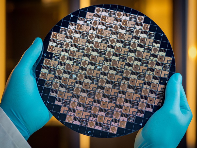
Fan-out Wafer Level Packaging (FOWLP) is one of the latest packaging trends in microelectronics. FOWLP has a high potential for significant package miniaturization concerning package volume but also its thickness. Technological core of FOWLP is the formation of a reconfigured molded wafer combined with a thin film redistribution layer to yield an SMD-compatible package. Main advantages of FOWLP are the substrateless package, low thermal resistance, improved RF performance due to shorter interconnects together with direct IC connection by thin film metallization instead of wire bonds or flip chip bumps and lower parasitic effects. Especially the inductance of FOWLP is much lower compared to FC-BGA packages. In addition, the redistribution layer can also provide embedded passives (R, L, C) as well as antenna structures using a multi-layer structure. Through mold vias (also called through polymer vias) can also be integrated. It can be used for multi-chip packages for system-in-package (SiP) and heterogeneous integration. For higher productivity and resulting lower cost larger mold embedding form factors are forecast for the near future. Besides increasing wafer diameter an alternative option would be moving to panel sizes leading to fan-out panel level packaging (FOPLP). Here, panel sizes could range from 18”x24” (a PCB manufacturing standard) to even larger sizes.
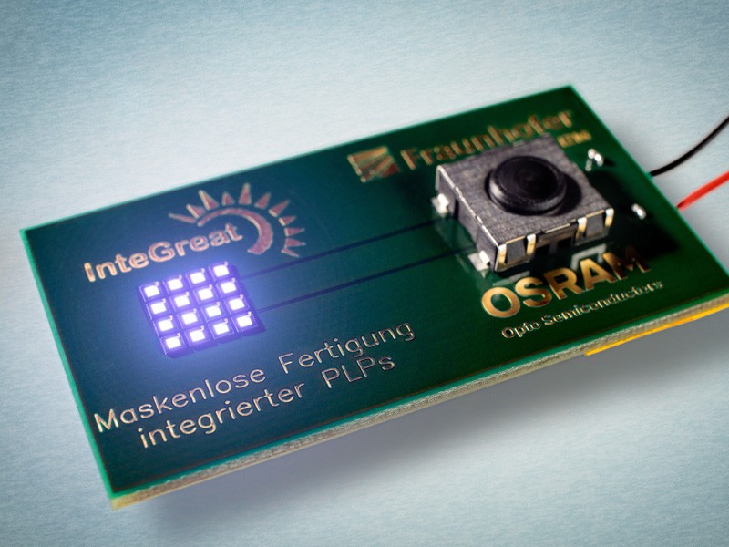
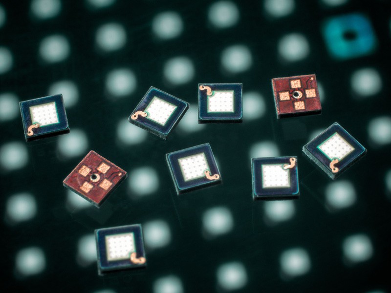
In cooperation with TU Berlin Fraunhofer IZM intensively works on both topics, in publicly funded projects as well as in direct industry cooperation. Within the H2020 project smart-MEMPHIS the goal is to design, manufacture and test a miniaturized autonomous energy supply consisting of a piezo-MEMS energy harvester, power management circuitry and energy storage. Target applications are a leadless pacemaker and structural health monitoring, the packaging technology of choice for maximum miniaturization is a fan-out panel level approach. Furthermore low cost technologies are developed in the BMBF-funded project “InteGreat”, also based on large area mold embedding. Industry projects are focusing among others on the evaluation of new materials for FOWLP for RF applications and process development for optical sensor systems. Derived from the activities a large industry consortium is planned to evolve fan-out panel level packaging together with partners along the value chain as well as end-users and OSATs (Outsourced Semiconductor Assembly and Test) to a higher productivity level.