Cost-effective and individualized advanced electronic packaging in small batches now available
Fraunhofer IZM is joining the EUROPRACTICE IC Service platform
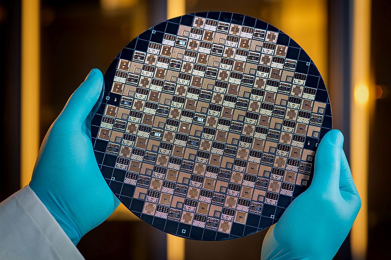
Fraunhofer IZM is joining the EUROPRACTICE IC Service platform. Together, the partners are making fan-out wafer level packaging (FOWLP) for electronic devices available and affordable even in small batches – and thus of interest to research institutes, universities, and SMEs. Costs can be significantly reduced by up to ten customers implementing individual fan-out wafer level packaging for their ICs or other components on a multi-project wafer. The target group includes any organization that does not produce in large quantities, but requires prototypes.
Research always means trying things out and daring to do new things. Research institutes, universities, and SMEs do not produce in large batches, but rather make small batches of innovative prototypes. The challenge is that manufacturing an electronic chip means applying an integrated circuit to a tiny semiconductor plate in extremely difficult production conditions – a very expensive process. The same applies to fan-out wafer level packaging. The multi-project wafer method can be of assistance here, too. Six to ten customers can join forces and produce different chips on a shared wafer. The development costs are shared and thus become more affordable. Instead of buying a whole bar of chocolate, you can get together with others and buy a box of chocolates – everyone pays his or her share of the price and gets the chocolate he or she likes.
This service is managed by the platform EUROPRACTICE IC Service The platform was founded in 1995 with the aim of helping small companies and research institutes to produce silicon chips in small quantities. Since 2019, Fraunhofer IZM has also been a member of the platform, and is able to expand its remit: in addition to the manufacture of electronic chips, advanced packaging using the multi-project wafer method is also an option.
The path to an individualized chip package
Anyone who needs packaging for fewer than 100 electronic components is in the target group. First of all, interested customers have to register on the Europractice website. A confidentiality agreement is signed and material data is then exchanged. The customer receives a set of slides with design guidelines on the basis of which he or she can design individualized packaging design in cooperation with Fraunhofer experts. “Special requests, such as a smaller package outline, are an option,” emphasizes Dr. Tanja Braun, group leader at Fraunhofer IZM, “but they cost extra. The electronic chips are then packaged in Fraunhofer IZM's clean rooms. After around four months, the customer receives his or her packaged chips.
The advantages are obvious: instead of paying the total cost of packaging an entire wafer, the customer only has to pay for the quantity he or she actually needs. For 20 to 30 chips, say, a customer only needs to pay a tenth of the price – and receives enough prototypes to carry out experiments. In addition, interested parties benefit from the latest packaging technology currently available on the market: fan-out wafer level packaging. The technological basis of the FOWLP is a reconfigured, molded wafer with embedded chips and a thin-film layer of surrounding wire, which together form an SMD-compatible package. The main advantages of the FOWLP are a very thin, substrate-less package, low thermal resistance and good RF characteristics due to short and planar electrical connections together with a bump-less chip connection instead of wire bonds or solder contacts.
The collaboration between EUROPRACTICE and Fraunhofer IZM will be launched this year with an early access run. Six to ten customers will share a wafer and thus be able to manufacture their prototypes at low cost. As Dr. Tanja Braun summarizes: “This will make individualized electronic packaging affordable for research institutes – so researchers will get some chocolates too!”
Last modified:
 Fraunhofer Institute for Reliability and Microintegration IZM