New Processes for Embedding Electronic Components in Large-Area Organic Substrates
PEKOS
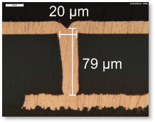
Microsection
The project is dedicated to the development of new processes and machines for a novel form of packaging in microelectronics: panel-level packaging. Combined circuit board and thin-film technologies are used to embed microchips and other electronic components into thin organic substrates, paving the way for the cost-efficient, large-scale production of complex modules with unprecedented levels of miniaturization possible.