We research integration technologies for system-in-package products, focusing in particular on device assembly for highly integrated packages and joining/encapsulation processes based on polymeric materials. Our technology portfolio includes pick-and-place processes – also for large-area substrates and 3D assemblies – and a wide variety of encapsulation processes, from dispensing and jetting to transfer and compression molding. Material, process and device analyses complete our range of expertise.

© Fraunhofer IZM | Volker Mai
Assembly and Encapsulation
Tabbed contents
Key Research Areas
Panel-level packaging
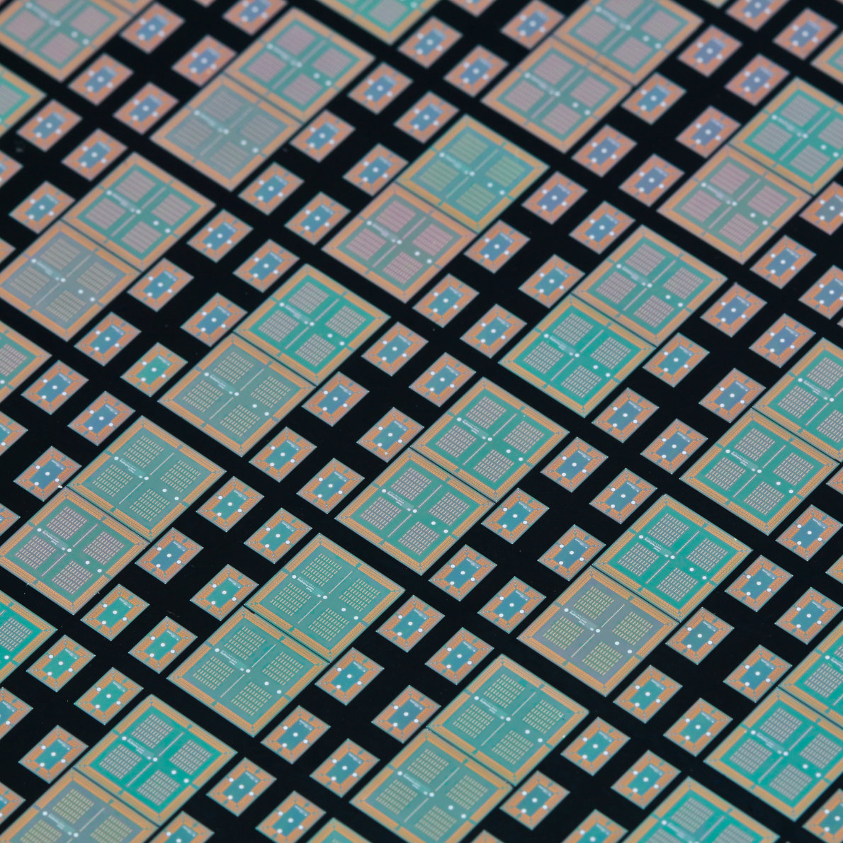
Developing demands and the market show two main trends helping to shape the ongoing development of system integration technologies. First of all is an ongoing increase in the number of functions directly included in a system — such as electrical, optical, mechanical, biological and chemical processes — combined with the demand for higher reliability and longer system lifetime. Second is the increasingly seamless merging of products and electronics, which necessitates adapting electronics to predefined materials, forms and application environments.
Fan-out wafer- panel level packaging

Fan-out Wafer Level Packaging (FOWLP) is one of the latest packaging trends in microelectronics. FOWLP has a high potential for significant package miniaturization concerning package volume but also its thickness. Technological core of FOWLP is the formation of a reconfigured molded wafer combined with a thin film redistribution layer to yield an SMD-compatible package.
Services
Balling for SiP / balling for interposer
Today’s packages with their high I/O counts call for high density interconnect schemes, typically a ball grid array configuration for SMT compatible mounting is used. Balling processes are also applied for Chiplet interposers, fan-in and fan-out wafer-level packages and for single die bumping. For the balling process solder preforms of different diameters (> 80 µm) and different alloys (SnAgCu, SnBi, Cu-core, …) are used.
Assembly
Material dosing
Process-oriented material analytics and process simulation
Development of technologies at Fraunhofer IZM is closely connected with process-oriented analytics of used materials. The investigations are focused on measurement of material characteristics under process conditions as well as systematic studies of aging processes of polymers under harsh environmental conditions.
Encapsulation
Protection of components by compression and transfer molding, underfilling, GlobTop, potting; production of reconfigurable wafers / panels with embedded chips by compression molding for Fan-Out Wafer and Panel-Level Packaging; production of 3D functional structures (incl. antennas) and 3D substrates by compression molding or direct metallization.
Reactive polymers are used primarily for encapsulation purposes. Typical choices include highly filled epoxy systems [EP] for molding, flip-chip underfilling, or GlobTop. Other polymer classes are available for specialized applications, e.g. highly thermally stable silicones [SI] for encapsulating power electronics or polyurethanes [PU] for potting assembled components.
Analysis
Materials, Processes, Components & Assemblies
Process analysis to support process development (by camera or high-speed camera) through in-line data capture (log files, additional sensor systems: sensor molding tool) and at-line material analysis (reaction behavior, viscosity etc.) or through the (non-destructive and destructive) analysis of finished systems.
Reliability analysis
Processes, Components & Assemblies
Assessment of process quality and stability; pre or post-load quality analysis in accordance with international standards (reflow stability, thermocycling, media resistance)
Projects
Development of Compression Molding Process for Encapsulation of Power Modules
Project Panel Power
Molding technology has been established as an encapsulation technology for power modules, but each module is encapsulated in a product-specific, single cavity and all contacts are in one plane, which requires subsequent forming of the signal pins. Fraunhofer IZM is introducing the encapsulation of power modules by compression molding. The process offers the advantage of using a height-flexible molding tool for the simultaneous encapsulation of multiple heterogeneous devices with different widths and/or thicknesses. In addition, less encapsulation material is used as compression molding is a runnerless process.

Supercomputing platform for fully automated vehicles
Project CeCaS
Fraunhofer IZM is contributing its expertise in the packaging of central car server chiplet modules on organic interposers. Our researchers are developing flip-chip assembly concepts and thermal interfaces for sustainable, scalable cooling concepts for this complex central car server. Derived from the research work on packaging, contributions are being made to the digital twin for the reliability assessment of chiplet-based electronic modules.
Trusted data acquisition in microelectronics manufacturing as a basis for ML-optimized processing
Project SiEvEI 4.0
In the digitization of manufacturing processes, one of the major goals is the connection of production facilities and the use of data to digitize business processes. In order to optimize manufacturing processes and maximize the quality of the resulting product, further process information and data directly from the work piece and from the manufacturing environment are required to achieve a holistic system view in addition to the selected data that the manufacturing systems already provide.

AI-powered radar solution for safe autonomous driving
Project KI-Radar
Come snow, rain, heat, or gloom of night - autonomous vehicles have to be safe on the road and work in every weather. In addition, they must be able to navigate routes with little traffic and few turns just as well as busy roads in urban areas. In order to detect potential obstacles and hazards, even those coming from the side, at an early stage, sensors are needed that enable 360° monitoring all around the vehicle. This requires extremely powerful and coordinated software and hardware components.

Reliable single chip package
Project
Fraunhofer IZM introduces a package alternative to commercially available PCB-based Power CSPs: a mold-embedded power die, addressing power electronics packages requirements as good thermal conduction to bottom and also to top; high thermal mass on top for Wide Band Gap short circuit capability and low production cost. Major difference to PCB-based single chip packages is the use of an isotropic isolating material.

Power module for Formula 1 with substrate water cooling
Project

Recovered by Robo Ray
Project RoboSkin
Giant arsenals of unexploded ordinance are sitting on the ocean floor, lost in battle or dumped as waste. The risky job of detecting these underwater hazards is currently given to submarines specially fitted for the purpose. But even they cannot get to some of the tighter or harder to reach spots, forcing expert divers to go down and take over the often life-threatening work. A German research consortium including Fraunhofer IZM is now using a submarine robot that is as nimble and mobile as a manta ray and equipped with innovative connected sensors on its fins to gather more information about its surroundings.

360° real-time capture: using 3D radar sensors to drive autonomously without blind spots
Project KoRRund
In order to be able to guarantee the highest level of safety in automated driving, 3D radar modules that can be positioned relatively freely on the vehicle and integrated into a sensor network, enabling 360° all-round vision, were developed by the KoRRund project. This allows them to analyze their environment in real time and from all perspectives simultaneously.

Universal sensor platform
Project USeP
Main focus of this project is a universal sensor platform. For the development of this USeP sensor package, state of the art technologies of the partners GlobalFoundries and several Fraunhofer Institutes is utilized. The package has two parts: one can be produced in advanced and includes basic core elements such as processor, memory or battery. In the second part, individually selectable sensors are included.

EuroPAT-MASIP
Project EuroPAT-MASIP
EuroPat-MASIP is committed to:
- Modelling, designing, and simulating packaging features and challenges in the field
- Key technologies for packaging, equipment, and materials
- Heterogeneous (3D) integration of smart system blocks (More-than-Moore, MtM) and SIP
- Metrology, methods and equipment, reliability, and weak spot testing procedures


Awards
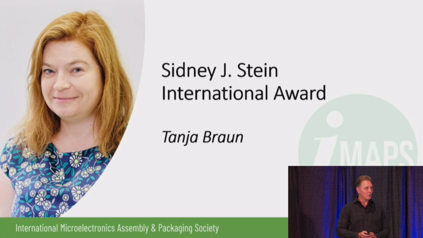
Dr. Tanja Braun receives the "Sydney Stein Award"
2021
Dr. Tanja Braun receives the „Exceptional Technical Achievement Award“ of the IEEE Electronics Packaging Society (EPS)
2021

PLP - A cost effective packaging platform for heterogeneous integration
Developing demands and the market show two main trends helping to shape the ongoing development of system integration technologies. First of all is an ongoing increase in the number of functions directly included in a system — such as electrical, optical, mechanical, biological and chemical processes — combined with the demand for higher reliability and longer system lifetime. Second is the increasingly seamless merging of products and electronics, which necessitates adapting electronics to predefined materials, forms and application environments.
